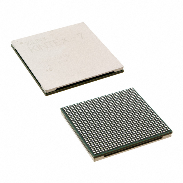
| Manufacturer Part#: | LFE2-6SE-5FN256C |
| Product Category: | Embedded - FPGAs (Field Programmable Gate Array) |
| Manufacturer: | Lattice Semiconductor |
| Description: | IC FPGA 190 I/O 256BGA |
| Package: | 256-BGA |
| Quantity: | 270 PCS |
| Lead Free Status / RoHS Status: | Lead free / RoHS Compliant |
| one to seven days | |
| Click buy button to purchase: | Buy |
CAD Models

LFE2-6SE-5FN256C Symbol

LFE2-6SE-5FN256C Footprint
Lifecycle Status Indicator

LFE2-6SE-5FN256C Lifecycle Status Indicator
Product Attributes
Manufacturer | Lattice Semiconductor Corporation |
Product Category | Embedded - FPGAs (Field Programmable Gate Array) |
Series | ECP2 |
Status | Active |
Brand | Lattice |
Lead Free | Lead Free |
REACH Compliant | Yes |
EU RoHS Compliant | Yes |
China RoHS Compliant | Yes |
Combinatorial Delay of a CLB-Max | 0.358 ns |
Dedicated DSP | 3 |
Device Number of DLLs/PLLs | 2+0+2 |
GMACs | 3.9 |
HTSUSA | 8542390001 |
JESD-30 Code | S-PBGA-B256 |
JESD-609 Code | e1 |
Mounting Style | SMD/SMT |
Mounting Type | Surface Mount |
Maximum Operating Temperature | 85 °C |
Minimum Operating Temperature | 0 °C |
Maximum Reflow Temperature | 250 °C |
Maximum Voltage Supply | 1.26 V |
Normal Supply Voltage | 1.2 V |
Minimum Voltage Supply | 1.14 V |
Maximum Operating Frequency | 311 MHz |
Maximum Distributed RAM Bits | 12288 |
Maximum Differential I/O Pairs | 95 |
Maximum I/O Performance | 3.125 Gbps |
Mega Multiply Accumulates per second | 3900 |
Memory Size | 67 Kb |
Number of I/Os | 100 |
Number of I/O Banks | 8 |
Number of Logic Blocks (LABs) | 750 |
Number of Logic Elements/Cells | 6000 |
Number of Pins | 256 |
Number of Multipliers | 12 (18x18) |
Embedded Memory | 55 Kbit |
Total Number of Block RAM | 3 |
Number of Inputs | 190 |
Number of Outputs | 190 |
Package / Case | 256-BGA |
Packaging | Tray |
Mfr Package Description | 17 X 17 MM, LEAD FREE, FPBGA-256 |
Package Length | 17 mm |
Package Width | 17 mm |
PackageHeight | 1.2 mm |
Seated Plane Height | 1.7 mm |
PCB changed | 256 |
Package Body Material | PLASTIC/EPOXY |
Package Code | BGA |
Package Equivalence Code | BGA256,16X16,40 |
Package Shape | SQUARE |
Package Style | GRID ARRAY |
Power Supplies | 1.2 |
Process Technology | 90 nm |
Programmable Logic Type | FIELD PROGRAMMABLE GATE ARRAY |
Program Memory Type | SRAM |
RAM Size | 55296b |
Shift Registers | Utilize LUT |
Speed Grade | 5 |
Subcategory | Programmable Logic ICs |
Supplier Device Package | 256-FPBGA (17x17) |
Tradename | LatticeEC |
Terminal Finish | Tin/Silver/Copper (Sn/Ag/Cu) |
Terminal Form | BALL |
Terminal Pitch | 1.0 mm |
Terminal Position | BOTTOM |
Time@Peak Reflow Temperature-Max (s) | 30 |
Features
◆ High Logic Density for System Integration
• 6K to 95K LUTs
• 90 to 583 I/Os
◆ Embedded SERDES (LatticeECP2M Only)
• Data Rates 250 Mbps to 3.125 Gbps
• Up to 16 channels per device PCI Express, Ethernet (1GbE, SGMII), OBSAI, CPRI and Serial RapidIO.
◆ sysDSP™ Block
• 3 to 42 blocks for high performance multiply and accumulate
• Each block supports – One 36x36, four 18x18 or eight 9x9 multipliers
◆ Flexible Memory Resources
• 55Kbits to 5308Kbits sysMEM™ Embedded Block RAM (EBR)
– 18Kbit block
– Single, pseudo dual and true dual port
– Byte Enable Mode support
• 12K to 202Kbits distributed RAM
– Single port and pseudo dual port
◆ sysCLOCK Analog PLLs and DLLs
• Two GPLLs and up to six SPLLs per device
– Clock multiply, divide, phase & delay adjust
– Dynamic PLL adjustment
• Two general purpose DLLs per device
◆ Pre-Engineered Source Synchronous I/O
• DDR registers in I/O cells
• Dedicated gearing logic
• Source synchronous standards support
– SPI4.2, SFI4 (DDR Mode), XGMII
– High Speed ADC/DAC devices
• Dedicated DDR and DDR2 memory support
– DDR1: 400 (200MHz) / DDR2: 533 (266MHz)
• Dedicated DQS support n
◆ Programmable sysI/O™ Buffer Supports Wide Range Of Interfaces
• LVTTL and LVCMOS 33/25/18/15/12
• SSTL 3/2/18 I, II
• HSTL15 I and HSTL18 I, II
• PCI and Differential HSTL, SSTL
• LVDS, RSDS, Bus-LVDS, MLVDS, LVPECL n
◆ Flexible Device Configuration
• 1149.1 Boundary Scan compliant
• Dedicated bank for configuration I/Os
• SPI boot flash interface
• Dual boot images supported
• TransFR™ I/O for simple field updates
• Soft Error Detect macro embedded n
◆ Optional Bitstream Encryption (LatticeECP2/M “S” Versions Only) n ◆ System Level Support
• ispTRACY™ internal logic analyzer capability
• On-chip oscillator for initialization & general use
• 1.2V power supply
Overview
The LatticeECP2/M family of FPGA devices is optimized to deliver high performance features such as advanced DSP blocks, high speed SERDES (LatticeECP2M family only) and high speed source synchronous interfaces in an economical FPGA fabric. This combination was achieved through advances in device architecture and the use of 90nm technology.
The LatticeECP2/M FPGA fabric is optimized with high performance and low cost in mind. The LatticeECP2/M devices include LUT-based logic, distributed and embedded memory, Phase Locked Loops (PLLs), Delay Locked Loops (DLLs), pre-engineered source synchronous I/O support, enhanced sysDSP blocks and advanced configuration support, including encryption (“S” versions only) and dual boot capabilities.
The LatticeECP2M device family features high speed SERDES with PCS. These high jitter tolerance and low transmission jitter SERDES with PCS blocks can be configured to support an array of popular data protocols including PCI Express, Ethernet (1GbE and SGMII), OBSAI and CPRI. Transmit Pre-emphasis and Receive Equalization settings make SERDES suitable for chip to chip and small form factor backplane applications.
Advantages and Disadvantages
There is no relevant information available for this part yet.
Applications
There is no relevant information available for this part yet.
ECCN / UNSPSC
ECCN | EAR99 |
USHTS | 8542310001 |
CAHTS | 8542310000 |
CNHTS | 8542310000 |
MXHTS | 85423199 |
TARIC | 8542319000 |
Documents & Media
Datasheet |
Product Manufacturer
Lattice Semiconductor (NASDAQ: LSCC) is the global leader in smart connectivity solutions, providing market leading intellectual property and low-power, small form-factor devices that enable more than 8,000 global customers to quickly deliver innovative and differentiated cost and power efficient products. The Company¹s broad end-market exposure extends from consumer electronics to industrial equipment, communications infrastructure and licensing.
Lattice was founded in 1983 and is headquartered in Portland, Oregon. The Company acquired Silicon Image in March 2015, which is a leader in setting industry standards including the highly successful HDMI®, DVI, MHL® and WirelessHD® standards.
Product Range
iCE40 Ultra/UltraLite | iCE40 UltraPlus | iCE40 LP/HX/LM |
MachXO3 | LatticeXP2 | ispMACH 4000ZE |
ECP5 & ECP5-5G | LatticeECP3 | LatticeECP2/M |
Lattice Diamond | Lattice Radiant | ispLEVER Classic |
Distributors
Distributors | Stock | Manufacturers | Descriptions |
Kynix | 270 | Lattice Semiconductor Corporation | IC FPGA 190 I/O 256BGA |
DigiKey | 1890 | Lattice Semiconductor Corporation | IC FPGA 190 I/O 256FBGA |
Mouser | 90 | Lattice | FPGA - Field Programmable Gate Array 6K LUTs 190 I/O S-Ser DSP 1.2V -5 |
Alternative Models
There is no relevant information available for this part yet.
Popularity by Region

LFE2-6SE-5FN256C Popularity by Region
Market Price Analysis

LFE2-6SE-5FN256C Market Price Analysis
 IC FPGA 68 I/O 100VQFP
 IC FPGA 48 I/O 63WLCSP
 IC FPGA 500 I/O 900FCBGA