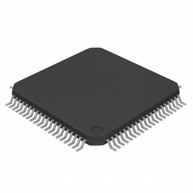
| Manufacturer Part#: | MCF51JE256CLK |
| Product Category: | Embedded - Microcontrollers |
| Manufacturer: | NXP |
| Description: | IC MCU 32BIT 256KB FLASH 80LQFP |
| Package: | 80-LQFP |
| Quantity: | 2091 PCS |
| Lead Free Status / RoHS Status: | Lead free / RoHS Compliant |
| one to seven days | |
| Click buy button to purchase: | Buy |
CAD Models
There is no relevant information available for this part yet.
Lifecycle Status Indicator

MCF51JE256CLK Lifecycle Status Indicator
Product Attributes
Manufacturer | Freescale Semiconductor - NXP |
Product Category | Embedded - Microcontrollers |
Status | Active |
Series | MCF51JE |
Mounting-Type | Surface Mount |
Brand | Freescale Semiconductor - NXP |
ADC Channels | 8 |
ADC Resolution | 12 bit |
Address Bus Width | 0.0 |
Analog Comparators | 1 |
Bit Size | 32 |
CPU Family | COLDFIRE |
Core Size | 32-Bit |
Core Processor | Coldfire V1 |
Core Architecture | ColdFire |
Connectivity | CANbus, EBI/EMI, I²C, SCI, SPI, USB OTG |
Clock Frequency-Max | 16.0 MHz |
China RoHS Compliant | Yes |
Device Core | ColdFire |
DAC Channels | 1 |
DAC Resolution | 12 bit |
DMA Channels | No |
Data Converters | A/D 12x12b; D/A 1x12b |
Data RAM Size | 32 kB |
Data Bus Width | 32 bit |
EEPROM Size | - |
EU RoHS Compliant | Yes |
External Data Bus Width | 0.0 |
Frequency | 50.33 MHz |
Family Name | MCF51JE |
Interface Type | I2C/SCI/SPI |
Instruction Set Architecture | RISC |
JESD-30 Code | S-PQFP-G80 |
JESD-609 Code | e3 |
Lead Finish | Matte Tin |
Lead Shape | Gull-wing |
Mounting Style | SMD/SMT |
Moisture Sensitivity Level | 3 |
Maximum Clock Rate | 50.33 MHz |
Maximum CPU Frequency | 50.33 MHz |
Maximum Clock Frequency | 50.3 MHz |
Number of I/Os | 47 |
Number of Pins | 80 |
Number of ADCs | Single |
Number of DACs | Single |
Number of Timers | 1 |
Number of PWM Channels | 8 |
Number of Programmable I/Os | 47 |
On-Chip ADC | 8-chx12-bit |
On-Chip DAC | 1-chx12-bit |
Oscillator Type | External |
Operating Temperature-Min | -40.0 ℃ |
Operating Temperature-Max | 85.0 ℃ |
PWM | 8 |
Pin Count | 80 |
PCB changed | 80 |
Peripherals | I2C, LVD, PWM, WDT |
Product Type | 32-bit Microcontrollers - MCU |
PWM Channels | Yes |
Power Supplies | 2/3.3 |
Package / Case | 80-LQFP |
Package Style | FLATPACK, LOW PROFILE, FINE PITCH |
Package Code | LFQFP |
Package Shape | SQUARE |
Package Body Material | PLASTIC/EPOXY |
Package Equivalence Code | QFP80,.55SQ,20 |
Programmability | Yes |
Program Memory Size | 256KB (256K x 8) |
Program Memory Type | FLASH |
Peak Reflow Temperature | 260 ℃ |
RAM Size | 32K x 8 |
RAM (bytes) | 32768.0 |
ROM (words) | 262144 |
ROM Programmability | FLASH |
Speed | 50.33 MHz |
Sub Category | Microcontrollers |
Surface Mount | Yes |
Seated Height-Max | 1.6 mm |
Supply Current-Max | 48.0 mA |
Supply Voltage-Nom | 3.0 V |
Supply Voltage-Min | 1.8 V |
Supply Voltage-Max | 3.6 V |
Supplier Device Package | 80-FQFP (12x12) |
Tradename | ColdFire |
Technology | CMOS |
Terminal Pitch | 0.5 mm |
Terminal Form | GULL WING |
Terminal Finish | Matte Tin (Sn) |
Terminal Position | QUAD |
Temperature Grade | INDUSTRIAL |
Time@Peak Reflow Temperature-Max | 40 s |
Voltage - Supply (Vcc/Vdd) | 1.8 V ~ 3.6 V |
Height | 1.4 mm |
Length | 12.0 mm |
Width | 12.0 mm |
Unit Weight | 0.017320 oz |
Watchdog | 1 |
Overview
The MCF51JE256 series devices are members of the low-cost, low-power, high-performance ColdFire V1 family of 32-bit microcontrollers (MCUs).
Features
32-Bit ColdFire V1 Central Processor Unit (CPU)
• Up to 50.33 MHz ColdFire CPU above 2.4 V and 40 MHz CPU above 2.1 V and 20 MHz CPU above 1.8 V across temperature range of -40°C to 105°C.
• ColdFire Instruction Set Revision C (ISA_C).
• 32-bit multiply and accumulate (MAC) supports signed or unsigned integer or signed fractional inputs.
On-Chip Memory
• 256 K Flash comprised of two independent 128 K flash arrays; read/program/erase over full operating voltage and temperature; allows interrupt processing while programming.
• 32 KB System Random-access memory (RAM).
• Security circuitry to prevent unauthorized access to RAM and Flash contents.
Power-Saving Modes
• Two ultra-low power stop modes. Peripheral clock enable register can disable clocks to unused modules to reduce currents.
• Time of Day (TOD) — Ultra low-power 1/4 sec counter with up to 64 sec timeout.
• Ultra-low power external oscillator that can be used in stop modes to provide accurate clock source to the TOD. 6 µs typical wake up time from stop3 mode.
Clock Source Options
• Oscillator (XOSC1) — Loop-control Pierce oscillator; 32.768 kHz crystal or ceramic resonator dedicated for TOD operation.
• Oscillator (XOSC2) for high frequency crystal input for MCG reference to be used for system clock and USB operations.
• Multipurpose Clock Generator (MCG) — PLL and FLL; precision trimming of internal reference allows 0.2% resolution and typical +0.5% to -1% deviation over temperature and voltage; supports CPU frequencies up to 50 MHz.
System Protection
• Watchdog computer operating properly (COP) reset with option to run from dedicated 1 kHz internal clock source or bus clock.
• Low-voltage detection with reset or interrupt; selectable trip points; separate low voltage warning with optional interrupt; selectable trip points.
• Illegal opcode and illegal address detection with reset.
• Flash block protection for each array to prevent accidental write/erasure.
• Hardware CRC to support fast cyclic redundancy checks.
Development Support
• Integrated ColdFire DEBUG_Rev_B+ interface with single wire BDM connection supports same electrical interface used by the S08 family debug modules.
• Real-time debug with 6 hardware breakpoints (4 PC, 1 address and 1 data).
• On-chip trace buffer provides programmable start/stop recording conditions.
Peripherals
• USB — Dual-role USB On-The-Go (OTG) device, supports USB in either device, host or OTG configuration. On-chip transceiver and 3.3V regulator help save system cost, fully compliant with USB Specification 2.0. Allows control, bulk, interrupt and isochronous transfers.
• SCIx — Two serial communications interfaces with optional 13-bit break; option to connect Rx input to PRACMP output on SCI1 and SCI2; High current drive on Tx on SCI1 and SCI2; wake-up from stop3 on Rx edge.
• SPI1 — Serial peripheral interface with 32-bit FIFO buffer; 16-bit or 8-bit data transfers; full-duplex or single-wire bidirectional; double-buffered transmit and receive; master or slave mode; MSB-first or LSB-first shifting.
• SPI2 — Serial peripheral interface with full-duplex or single-wire bidirectional; Double-buffered transmit and receive; Master or Slave mode; MSB-first or LSB-first shifting.
• IIC — Up to 100 kbps with maximum bus loading; Multi-master operation; Programmable slave address; Interrupt driven byte-by-byte data transfer; supports broadcast mode and 10-bit addressing.
• CMT — Carrier Modulator timer for remote control communications. Carrier generator, modulator and driver for dedicated infrared out (IRO). Can be used as an output compare timer.
• TPMx — Two 4-channel Timer/PWM Module; Selectable input capture, output compare, or buffered edge- or center-aligned PWM on each channel; external clock input/pulse accumulator.
• Mini-FlexBus — Multi-function external bus interface with user programmable chip selects and the option to multiplex address and data lines.
• PRACMP — Analog comparator with selectable interrupt; compare option to programmable internal reference voltage; operation in stop3.
• ADC12 — 12-bit Successive approximation ADC with up to12 single-ended channels; internal bandgap reference channel; operation in stop3; fully functional from 3.6V to 1.8V.
• PDB — Programmable delay block with 16-bit counter and modulus and prescale to set reference clock to bus divided by 1 to bus divided by 2048; 8 trigger outputs for ADC module provides periodic coordination of ADC sampling sequence with sequence completion interrupt; Back-to-Back mode and Timed mode.
• DAC — 12-bit resolution DAC; configurable settling time.
Input/Output
• Up to 68 GPIOs and 1 output-only pin.
• Voltage Reference output (VREFO).
• Dedicated infrared output pin (IRO) withhigh current sink capability.
• Up to 16 KBI pins with selectable polarity.
• Up to 16 pins of rapid general purpose I/O (RGPIO).
Advantages and Disadvantages
There is no relevant information available for this part yet.
Applications
There is no relevant information available for this part yet.
Compliance
USHTS: | 8542310001 |
CAHTS: | 8542310000 |
CNHTS: | 8542319000 |
JPHTS: | 8542310324 |
KRHTS: | 8542311000 |
MXHTS: | 85423199 |
TARIC: | 8542319000 |
RoHS: | Compliance |
Lead Free: | Lead Free |
Halogen Free: | Halogen Free |
REACH SVHC: | No SVHC |
Radiation Hardening: | No |
ECCN / UNSPSC
ECCN: | EAR99 |
HTSN: | 8542310001 |
SCHEDULE B: | 8542310000 |
Documents & Media
Datasheet | |
Environmental Information | |
PCN Design/Specification | |
Test/Quality Data | |
Product Manufacturer
NXP Semiconductor enables secure connections and infrastructure for a smarter world, advancing solutions that make lives easier, better and safer. As the world leader in secure connectivity solutions for embedded applications, NXP is driving innovation in the secure connected vehicle, end-to-end security & privacy and smart connected solutions markets. Built on more than 60 years of combined experience and expertise, the company has 45,000 employees in more than 35 countries.
Product Range
ARM ® PROCESSORS | ANALOG | POWER ARCHITECTURE ®PROCESSORS |
MEDIA AND AUDIO | RF | IDENTIFICATION & SECURITY |
Sensors | Wireless | Automotive Products |
Distributors
Distributors | Stock | Manufacturers | Descriptions |
Kynix | 2091 | Freescale Semiconductor - NXP | IC MCU 32BIT 256KB FLASH 80LQFP |
DigiKey | 0 | NXP USA Inc. | IC MCU 32BIT 256KB FLASH 80FQFP |
Mouser | 480 | NXP Semiconductors | 32-bit Microcontrollers - MCU FLASH-NON-ANALOG IP 256K |
Alternative Models
There is no relevant information available for this part yet.
Popularity by Region

MCF51JE256CLK Popularity by Region
Market Price Analysis
There is no relevant information available for this part yet.
Pictures

MCF51JE256CLK Images
 IC MCU 32BIT 256KB FLASH 100LQFP
 IC MCU 8BIT 1.75KB FLASH 8DFNS
 IC MCU 8BIT 8KB FLASH 8SOIC