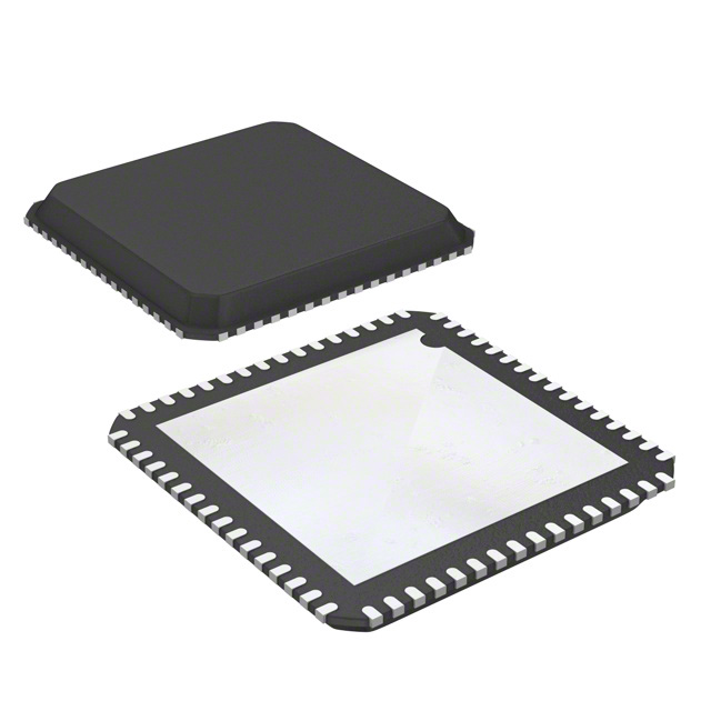
| Manufacturer Part#: | MCF52110CEP66 |
| Product Category: | Embedded - Microcontrollers |
| Manufacturer: | NXP |
| Description: | IC MCU 32BIT 128KB FLASH 64QFN |
| Package: | 64-VFQFN Exposed Pad |
| Quantity: | 1128 PCS |
| Lead Free Status / RoHS Status: | Lead free / RoHS Compliant |
| one to seven days | |
| Click buy button to purchase: | Buy |
CAD Models

MCF52110CEP66 Symbol

MCF52110CEP66 Footprint
Lifecycle Status Indicator

MCF52110CEP66 Lifecycle Status Indicator
Product Attributes
Manufacturer: | Freescale Semiconductor - NXP |
Product Category: | Embedded - Microcontrollers |
Series: | MCF521xx |
Mounting-Type: | Surface Mount |
Brand: | Freescale Semiconductor - NXP |
ADC Resolution: | 12 bit |
Bit Size | 32 |
Core Size | 32-Bit |
Core Processor | Coldfire V2 |
CPU Family | COLDFIRE |
Connectivity | I²C, SPI, UART/USART |
Clock Frequency-Max | 66.0 MHz |
Device Core | ColdFire |
Data RAM Size | 16 kB |
Data Bus Width | 32 bit |
EEPROM Size | - |
EU RoHS Compliant | Yes |
Interface Type | I2C/SPI/UART |
Instruction Set Architecture | RISC |
JESD-30 Code | S-PQCC-N64 |
JESD-609 Code | e3 |
Lead Finish | Matte Tin |
Mounting-Style | SMD/SMT |
Moisture Sensitivity Level | 3 |
Maximum Expanded Memory Size | 4 GB |
Maximum Operating Supply Voltage | 3.6 V |
Minimum Operating Supply Voltage | 3 V |
Number of Timers | 10 |
Number of I/Os | 43 |
Number of Pins | 64 |
Number of Terminals | 64 |
Number of ADC Channels | 8 |
On-Chip ADC | 8-chx12-bit |
Oscillator Type | Internal |
Operating Temperature-Min | -40.0 ℃ |
Operating Temperature-Max | 85.0 ℃ |
Pin Count | 64 |
Packaging | Tray |
Peripherals | DMA, LVD, POR, PWM, WDT |
Power Supplies | 3/3.3 |
Product Type | 32-bit Microcontrollers - MCU |
Package Body Material | PLASTIC/EPOXY |
Package Code | QCCN |
Package / Case | 64-VFQFN Exposed Pad |
Package Equivalence Code | LCC64,.35SQ,20 |
Package Shape | SQUARE |
Package Style | CHIP CARRIER |
Program Memory Size | 128KB |
Program Memory Type | FLASH |
Peak Reflow Temperature | 260 ℃ |
RAM (bytes) | 16384.0 |
RAM Size | 16K x 8 |
ROM Programmability | FLASH |
ROM (words) | 131072 |
REACH Compliant: | Yes |
Speed | 66.0 MHz |
Sub Category | Microcontrollers |
Supplier Package | QFN |
Supplier Device Package | 64-QFN-EP (9x9) |
Supply Voltage-Nom | 3.3 V |
Supply Voltage-Min | 3.0 V |
Supply Voltage-Max | 3.6 V |
Surface Mount | Yes |
Technology | CMOS |
Tradename | ColdFire |
Terminal Form | NO LEAD |
Terminal Pitch | 0.5 mm |
Terminal Finish | Matte Tin (Sn) |
Terminal Position | QUAD |
Temperature Grade | INDUSTRIAL |
Time@Peak Reflow Temperature-Max | 40 s |
Voltage - Supply (Vcc/Vdd) | 3 V ~ 3.6 V |
Height | 0.85 mm |
Length | 9.0 mm |
Width | 9.0 mm |
Watchdog | 1 |
Unit Weight | 0.006773 oz |
Overview
The MCF52211 microcontroller family is a member of the ColdFire® family of reduced instruction set computing (RISC) microprocessors. This document provides an overview of the 32-bit MCF52211 microcontroller, focusing on its highly integrated and diverse feature set.
This 32-bit device is based on the Version 2 ColdFire core operating at a frequency up to 80 MHz, offering high performance and low power consumption. On-chip memories connected tightly to the processor core include up to 128 Kbytes of flash memory and 16 Kbytes of static random access memory (SRAM).
Features
• Version 2 ColdFire variable-length RISC processor core
— Static operation
— 32-bit address and data paths on-chip
— Up to 80 MHz processor core frequency
— 40 MHz and 33 MHz off-platform bus frequency
— Sixteen general-purpose, 32-bit data and address registers
— Implements ColdFire ISA_A with extensions to support the user stack pointer register and four new instructions for improved bit processing (ISA_A+)
— Multiply-Accumulate (MAC) unit with 32-bit accumulator to support 16*16→32 or 32*32→32 operations
• System debug support
— Real-time trace for determining dynamic execution path
— Background debug mode (BDM) for in-circuit debugging (DEBUG_B+)
— Real-time debug support, with six hardware breakpoints (4 PC, 1 address and 1 data) configurable into a 1- or 2-level trigger
• On-chip memories
— Up to 16-Kbyte dual-ported SRAM on CPU internal bus, supporting core and DMA access with standby power supply support
— Up to 128 Kbytes of interleaved flash memory supporting 2-1-1-1 accesses
• Power management
— Fully static operation with processor sleep and whole chip stop modes
— Rapid response to interrupts from the low-power sleep mode (wake-up feature)
— Clock enable/disable for each peripheral when not used (except backup watchdog timer)
— Software controlled disable of external clock output for low-power consumption
• Universal Serial Bus On-The-Go (USB OTG) dual-mode host and device controller
— Full-speed / low-speed host controller
— USB 1.1 and 2.0 compliant full-speed / low speed device controller
— 16 bidirectional end points
— DMA or FIFO data stream interfaces
— Low power consumption
— OTG protocol logic
• Three universal asynchronous/synchronous receiver transmitters (UARTs)
— 16-bit divider for clock generation
— Interrupt control logic with maskable interrupts
— DMA support
— Data formats can be 5, 6, 7 or 8 bits with even, odd, or no parity
— Up to two stop bits in 1/16 increments
— Error-detection capabilities
— Modem support includes request-to-send (RTS) and clear-to-send (CTS) lines for two UARTs
— Transmit and receive FIFO buffers
• Two I2C modules
— Interchip bus interface for EEPROMs, LCD controllers, A/D converters, and keypads
— Fully compatible with industry-standard I2C bus
— Master and slave modes support multiple masters
— Automatic interrupt generation with programmable level
• Queued serial peripheral interface (QSPI)
— Full-duplex, three-wire synchronous transfers
— Up to four chip selects available
— Master mode operation only
— Programmable bit rates up to half the CPU clock frequency
— Up to 16 pre-programmed transfers
• Fast analog-to-digital converter (ADC)
— Eight analog input channels
— 12-bit resolution
— Minimum 1.125 μs conversion time
— Simultaneous sampling of two channels for motor control applications
— Single-scan or continuous operation
— Optional interrupts on conversion complete, zero crossing (sign change), or under/over low/high limit
— Unused analog channels can be used as digital I/O
• Four 32-bit timers with DMA support
— 12.5 ns resolution at 80 MHz
— Programmable sources for clock input, including an external clock option
— Programmable prescaler
— Input capture capability with programmable trigger edge on input pin
— Output compare with programmable mode for the output pin
— Free run and restart modes
— Maskable interrupts on input capture or output compare
— DMA trigger capability on input capture or output compare
• Four-channel general purpose timer
— 16-bit architecture
— Programmable prescaler
— Output pulse-widths variable from microseconds to seconds
— Single 16-bit input pulse accumulator
— Toggle-on-overflow feature for pulse-width modulator (PWM) generation
— One dual-mode pulse accumulation channel
• Pulse-width modulation timer
— Support for PCM mode (resulting in superior signal quality compared to conventional PWM)
— Operates as eight channels with 8-bit resolution or four channels with 16-bit resolution
— Programmable period and duty cycle
— Programmable enable/disable for each channel
— Software selectable polarity for each channel
— Period and duty cycle are double buffered. Change takes effect when the end of the current period is reached (PWM counter reaches zero) or when the channel is disabled.
— Programmable center or left aligned outputs on individual channels
— Four clock sources (A, B, SA, and SB) provide for a wide range of frequencies
— Emergency shutdown
• Two periodic interrupt timers (PITs)
— 16-bit counter
— Selectable as free running or count down
• Real-Time Clock (RTC)
— Maintains system time-of-day clock
— Provides stopwatch and alarm interrupt functions
• Software watchdog timer
— 32-bit counter
— Low-power mode support
• Backup watchdog timer (BWT)
— Independent timer that can be used to help software recover from runaway code
— 16-bit counter
— Low-power mode support
• Clock generation features
— Crystal, on-chip trimmed relaxation oscillator, or external oscillator reference options
— Trimmed relaxation oscillator
— Pre-divider capable of dividing the clock source frequency into the PLL reference frequency range
— System can be clocked from PLL or directly from crystal oscillator or relaxation oscillator
— Low power modes supported
— 2n (0≤n≤15) low-power divider for extremely low frequency operation
• Interrupt controller
— Uniquely programmable vectors for all interrupt sources
— Fully programmable level and priority for all peripheral interrupt sources
— Seven external interrupt signals with fixed level and priority
— Unique vector number for each interrupt source
— Ability to mask any individual interrupt source or all interrupt sources (global mask-all)
— Support for hardware and software interrupt acknowledge (IACK) cycles
— Combinatorial path to provide wake-up from low-power modes
• DMA controller
— Four fully programmable channels
— Dual-address transfer support with 8-, 16-, and 32-bit data capability, along with support for 16-byte (4*32-bit) burst transfers
— Source/destination address pointers that can increment or remain constant
— 24-bit byte transfer counter per channel
— Auto-alignment transfers supported for efficient block movement
— Bursting and cycle-steal support
— Software-programmable DMA requests for the UARTs (3) and 32-bit timers (4)
• Reset
— Separate reset in and reset out signals
— Seven sources of reset:
– Power-on reset (POR)
– External
– Software
– Watchdog
– Loss of clock / loss of lock
– Low-voltage detection (LVD)
– JTAG
— Status flag indication of source of last reset
• Chip configuration module (CCM)
— System configuration during reset
— Selects one of six clock modes
— Configures output pad drive strength
— Unique part identification number and part revision number
• General purpose I/O interface
— Up to 56 bits of general purpose I/O
— Bit manipulation supported via set/clear functions
— Programmable drive strengths
— Unused peripheral pins may be used as extra GPIO
• JTAG support for system level board testing
Advantages and Disadvantages
There is no relevant information available for this part yet.
Applications
There is no relevant information available for this part yet.
Compliance
USHTS: | 8542310001 |
CNHTS: | 8542319000 |
JPHTS: | 8542310324 |
MXHTS: | 85423199 |
TARIC: | 8542319000 |
Lead Free: | Lead Free |
Halogen Free: | Halogen Free |
RoHS: | Compliance |
Radiation Hardening: | No |
ECCN / UNSPSC
ECCN: | 3A991.A.2 |
HTSN: | 8542310001 |
SCHEDULE B: | 8542310000 |
Documents & Media
Datasheet | |
PCN Obsolescence/ EOL | |
Test/Quality Data | |
Product Manufacturer
NXP Semiconductors enables secure connections and infrastructure for a smarter world, advancing solutions that make lives easier, better and safer. As the world leader in secure connectivity solutions for embedded applications, NXP is driving innovation in the secure connected vehicle, end-to-end security & privacy and smart connected solutions markets. Built on more than 60 years of combined experience and expertise, the company has 45,000 employees in more than 35 countries.
Product Range
ARM ® PROCESSORS | ANALOG | POWER ARCHITECTURE ®PROCESSORS |
MEDIA AND AUDIO | RF | IDENTIFICATION & SECURITY |
Sensors | Wireless | Automotive Products |
Distributors
Distributors | Stock | Manufacturers | Descriptions |
Kynix | 1128 | Freescale Semiconductor - NXP | IC MCU 32BIT 64KB FLASH 64QFN |
DigiKey | 0 | NXP USA Inc. | IC MCU 32BIT 64KB FLASH 64QFN |
Mouser | 0 | NXP / Freescale | 32-bit Microcontrollers - MCU KIRIN0 WITHOUT USB |
Alternative Models
There is no relevant information available for this part yet.
Popularity by Region

Market Price Analysis
There is no relevant information available for this part yet.
Pictures

MCF52110CEP66 Images
 IC MCU 32BIT 256KB FLASH 100LQFP
 IC MCU 8BIT 1.75KB FLASH 8DFNS
 IC MCU 8BIT 8KB FLASH 8SOIC