20
Catalog
I Introduction | |
II Classification of Thyristor | 1. Classification by Turnoff, Conduction and Control Modes |
2. Classification by Pin and Polarity | |
3. Classification by Package Type | |
4.Classification by Current Capacity | |
5. Classification by Turn-off Speed | |
III Working Process of Thyristor | |
IV Gate turn-off Thyristor | 1. The Differences between GTO and SCR |
2. Detection of GTO | |
V How to Protect Thyristor? | 1. Overvoltage Protection(OVP) |
2. Overcurrent Protection | |
I Introduction
Thyristor is the abbreviation of thyratron transistor, which is also known as silicon controlled rectifier. In 1957, General Electric Company developed the world's first thyristor product, and in 1958 made it commercialized.
The structure of thyristor is a PNPN four-layer semiconductor structure, which has three poles: anode, cathode and gate pole. Its working conditions are: a forward voltage is added and there is a trigger current at the gate pole. Its derived devices include fast thyristor, bidirectional thyristor, reverse conducting thyristors, light-controlled thyristors, etc.
It is a high-power switching semiconductor device, which is represented by the letter symbols "V" and "VT" in the circuit. The thyristor has the characteristics of a silicon rectifier device, which can work under high voltage and high current conditions. As its working process can be controlled, it’s widely used in controllable rectification, AC voltage regulation, non-contact electronic switching, inverter, frequency conversion and other electronic circuits.
What is a Thyristor?
II Classification of Thyristor
1. Classification by Turnoff, Conduction and Control Modes
According to the turnoff, conduction and control modes of the thyristors, they can be divided into ordinary thyristors, bidirectional thyristors, reverse conducting thyristors, gate-turn-off thyristors thyristors (GTO), BTG thyristors, temperature-controlled thyristors, and light-controlled thyristors.
2. Classification by Pin and Polarity
Thyristors can be divided into two-pole thyristors, three-pole thyristors and four-pole thyristors according to their pins and polarities.
3. Classification by Package Type
According to the package type of the thyristors, they can be classified into three groups: metal package thyristors, plastic package thyristors, and ceramic package thyristors. Among them, metal-encapsulated thyristors are divided into bolt-shaped, flat-shaped, and round-shell-shaped, etc.. And plastic-encapsulated thyristors are divided into types with or without cooling fins.
4. Classification by Current Capacity
Thyristors can be divided into high power thyristors, medium power thyristors and low power thyristors according to their current capacity. Generally, high-power thyristors are mostly packaged in metal casing, while medium- and low-power thyristors are mostly sealed in plastic or ceramic packages.
5. Classification by Turn-off Speed
Thyristors can be divided into ordinary thyristors and high-frequency (fast) thyristors according to their turn-off speed.
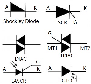
FIG1. Types of Thyristors
III Working Process of Thyristor
Thyristor is a four-layer three-terminal device. It has three PN junctions, J1, J2, and J3. The NP in the middle can be divided into two parts to form a PNP-type transistor and an NPN-type transistor.
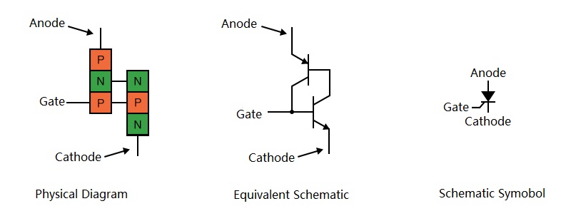
FIG2. Structure of Thyristor
When the thyristor is bearing the forward anode voltage, in order to turn on the thyristor, the PN junction J2 that withstands the reverse voltage must lose its blocking effect. Therefore, when there is enough gate current Ig flowing into the two-transistor circuits that are compounded with each other, a strong positive feedback will be formed, causing the two transistors to be saturated and conducted.
Set the collector currents of the PNP and NPN tubes be Ic1 and Ic2, the emitter currents be Ia and Ik, the current amplification factors be:
a1 = Ic1 / Ia and a2 = Ic2 / Ik,
and the reverse leakage current through the J2 junction is Ic0.
The anode current of the thyristor is equal to the sum of the collector current and the leakage current of the two tubes:
Ia = Ic1 + Ic2 + Ic0 or Ia = a1Ia + a2Ik + Ic0
If the gate current is Ig, the thyristor cathode current is Ik = Ia + Ig
And it can be concluded that the anode current of the thyristor is:
I = (Ic0 + Iga2) / (1- (a1 + a2)) Formula (1-1)
The current amplification factors a1 and a2 of the silicon PNP tube and silicon NPN tube change sharply with the change of their emitter currents.
When the thyristor is subjected to the forward anode voltage and the gate pole is not receiving voltage, in the formula (1-1), Ig = 0 and (a1 + a2) is very small, so the anode current of the thyristor Ia≈Ic0, and the thyristor is in the forward blocking state. When the thyristor is under the positive anode voltage, the current Ig flows from the gateG.
Because a sufficient amount of Ig flows through the emitter junction of the NPN tube, thereby increasing the start current amplification factor a2. And a sufficiently large electrode current Ic2 flows through the emitter juncture of the PNP tube, which increases the current amplification factor a1, resulting in a larger electrode current Ic1 flowing through the emitter junction of the NPN tube. This strong positive feedback process proceeds quickly.
When a1 and a2 increase as the emitter current increases and (a1 + a2) ≈ 1, the denominator in equation (1-1 ) 1- (a1 + a2) ≈ 0 , thus increasing the anode current Ia of the thyristor. At this time, the current flowing through the thyristor is completely determined by the voltage and resistance of the main circuit, and the thyristor is already in the forward conduction state.
In the formula (1-1), after the thyristor is turned on, 1- (a1 + a2) ≈ 0, and even if the gate current Ig = 0 at this time, the thyristor can maintain the original anode current Ia and continue to be turned on. After the thyristor is conducted, the gate is out of action.
After the thyristor is turned on, if the power supply voltage is continuously reduced or the loop resistance is increased to reduce the anode current Ia below the holding current IH, since a1 and a1 decrease rapidly, when 1- (a1 + a2) ≈ 0 , The thyristor return to the blocking state.
How does a Thyristor work?
IV Gate turn-off Thyristor
1. The Differences between GTO and SCR
Gate turn-off thyristor(GTO) is also known as gate-controlled thyristor. Its main characteristic is that when the gate pole is added a negative trigger signal, the thyristor can turn itself off.
As mentioned earlier, after the ordinary thyristor (SCR) is triggered by the positive gate signal, the signal can be maintained in the on-state. In order to turn it off, the power must be cut off or the reverse voltage is applied, so that the forward current is lower than the holding current. This needs to increase the commutating circuit, which not only increases the volume and weight of the device, but also reduces the efficiency and generates waveform distortion and noise.
The GTO thytristor overcomes the above drawbacks. It retains the advantages of high voltage proof and high current of ordinary thyristors, and has self-shutdown capability, which makes it very easy to use and be an ideal high-voltage and large-current switching device. Its capacity and service life exceed the giant transistor (GTR), but the operating frequency is lower than the GTR. The capacity of GTO has reached 3000A-4500V, and have been widely used in fields such as chopper speed control, frequency control, and inverter power supply, showing strong vitality.
GTO thytristor is also a PNPN four-layer three-terminal device, and its structure and equivalent circuit are the same as ordinary thyristors.
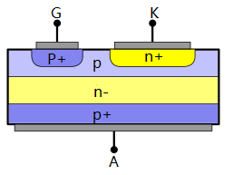
FIG3. Simplified Cross Section of a GTO Thyristor
Although the principle of GTO and SCR triggering is the same, the turnoff principle and method of the two are completely different. This is because ordinary thyristors are in a deeply saturated state after being turned on, and GTO can only reach critical saturation after being turned on, so the GTO gate pole can be turned off after we add a negative trigger signal on it.
An important parameter of GTO is the turn-off gain, βoff, which is equal to the ratio of the maximum off-state current of the anode to the maximum negative current of the gate. The formula is:
βoff = IATM / IGM
βoff is generally several times to several tens times. The larger the βoff is, the stronger the ability of the gate current to control the anode current will be.
2. Detection of GTO
(1) Determine the Electrode of GTO
Set the multimeter to the “R×1” gear and measure the resistance between any two pins. Only when the black test lead is connected to the G pole and the red test lead is connected to the K pole, the resistance is low. In other cases, the resistance value is infinite. This can quickly determine the G and K poles, and the rest is the A pole.
(2) Check the Triggering Capability
First connect the black test lead of the multimeter1 to the A pole and the red test lead to the K pole, the resistance is infinite. Then use the tip of the black test lead to contact the G pole at the same time, and add a positive trigger signal, if the pointer deflected to a low resistance value, it indicates that the GTO has been turned on. Finally, when the G pole is disconnected, as long as the GTO still in the on state, it means that it has the triggering ability.
(3) Check the Turnoff Capability
Double-meter method is used to check the shutdown capability. The gears and connections of multimete1 remain unchanged. Set the multimeter2 to “R×10” gear, connect the red test lead to the G pole, and the black test lead to the K pole, and apply a negative trigger signal to it. If the pointer of multimeter1 is turned to the left to the infinity position, it proves that the GTO has the ability to shut down.
(4) Estimated Turnoff Gain βoff
When proceeding to step 3, do not connect to multimeter2. Firstly note down the number of deflection grids n1 of multimeter1 on forward direction when GTO is turned on. Then connect to multimeter2 to force GTO to turn off, and note down the number of deflection grids n2 of multimeter2. Finally, read the current value, and the shutdown gain is estimated according to teh formula as follows:
βoff = IATM / IGM≈IAT / IG = K1n1 / K2n2
In the formula,
K1—current scale coefficient in “R×1” gear of multimeter1;
K2—current scale coefficient in “R×10” gear of multimeter2.
βoff≈10×n1 / n2
In this way, without calculating the values of IAT and IG, the turnoff gain value can be quickly estimated as long as we get the number of deflection grids.
V How to Protect Thyristors?
Nowadays, thyristors are becoming more and more widely used in industries. And with the increasing of application scope, the role of thyristors is becoming more and more comprehensive. However, in the using process, the thyristor is very sensitive to overvoltage, which could cause great damages. In order to ensure the service life of the thyristor, what can we do to better protect it? The protection methods are introduced as follows:
1. Overvoltage Protection(OVP)
The thyristor is very sensitive to overvoltage. When the forward voltage exceeds a certain value of the repetitive peak off-state voltage(UDRM), the thyristor will be turned on incorrectly, causing a circuit failure. When the applied reverse voltage exceeds a certain value of the reverse repetitive peak voltage(URRM), it will be damaged immediately. Therefore, it is necessary to study the cause of overvoltage and the method of suppressing overvoltage.
Overvoltage is mainly caused by drastic changes in the supplied electric power or the energy storage of the system, which makes the system not have enough time to convert, or the electromagnetic energy originally accumulated in the system not timely dissipate.
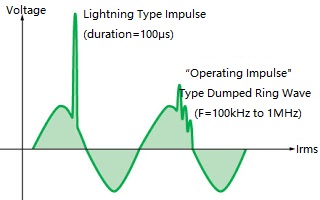
FIG4. Example of Overvoltage
(1) Types of Overvoltage
There are mainly two types of overvoltage: one is caused by external shocks such as lightning strikes, and the other is the impulse voltage caused by opening and closing of switches. The overvoltage generated by lightning strikes or the operation of high-voltage circuit breakers is a voltage spike of several microseconds to several milliseconds, which is very dangerous for thyristors. And the impulse voltage caused by the opening and closing of the switches is divided into the following categories:
1) Overvoltage Generated by the Open and Close of AC Power Supply
The overvoltage could be caused by the opening and closing of the AC switches or the fusing of the AC fuse protectors. Due to the distributed capacitance of the transformer winding, the resonance circuit caused by the leakage reactance, the overvoltage value becomes 2 to 10 times the normal value. Generally, the faster the opening and closing speed is, the higher the overvoltage will be, and the value will be even higher when the circuit is disconnected under no-load conditions.
2) Overvoltage Generated on the DC Side
If the inductance of the circuit is large or the current value when we cut off the circuit is large, a relatively large overvoltage will be generated. This situation often occurs when the current is abruptly changed, which is caused by cutting off the loads, the opening of the conducting thyristor or the fast fusing of the fuse protector.
3) Commutation Impulse Voltage
The commutation overvoltage is caused by the residual carrier recombination in the junction layers of the device when the current of the thyristor drops to 0, so it is also called the overvoltage caused by the carrier accumulation effect.
After commutation overvoltage, commutation oscillation overvoltage occurs. It is the oscillation voltage caused by the resonance of the inductance and capacitance. Its value is related to the reverse voltage after commutation. The higher the reverse voltage is, the greater the commutation oscillation overvoltage will be.
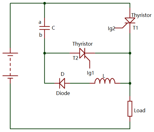
FIG5. Class D: Impulse Commutation
(2) Methods for Overvoltage
For different reasons for the formation of overvoltage, different suppression methods can be adopted, such as reducing the overvoltage source and attenuating the overvoltage amplitude; suppressing the rising rate of overvoltage energy, delaying the dissipation rate of the generated energy, and increasing its dissipation path; use electronic circuits for protection.
The most common method is to connect energy absorbing elements in the loop to dissipate the energy, which is often called an absorption loop or a buffer circuit.
1) Resistance-capacitance(RC) Snubber Circuit
Generally, the overvoltage has a high frequency, so capacitors are often used as absorber elements. To prevent oscillation, a damping resistor is often added to form a resistance-capacitance absorption circuit. The resistance-capacitance absorption circuit can be connected on the AC side and DC side of the circuit, or connected in parallel between the anode and the cathode of the thyristor. It is best to use non-inductive capacitors for the absorption circuit, and the wiring should be as short as possible.
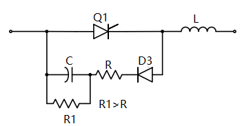
FIG6. Reverse Polarized RC Snubber Circuit
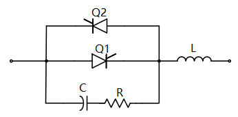
FIG7. An Un-polarized Snubber Circuit
2) Absorption Loop Composed of Non-linear Elements
The time constant RC of the resistance-capacitance absorption circuit above is fixed, and sometimes it can’t discharge the overvoltage with short time, high peak value, and large energy, and the effect of suppressing overvoltage is poor. Therefore, generally, non-linear components such as selenium stacks or varistors are also connected in parallel at the input and output lines of the converter.
The operating voltage of the selenium stack is related to temperature, and the lower the temperature is, the higher the withstand voltage will be. In addition, the selenium stack has a self-recovering property and can be used repeatedly. After the action of overvoltage, the burnt holes on the selenium substrate are covered again by the dissolved selenium, and the working characteristics are restored again.
The varistor is a metal oxide non-linear resistor based on zinc oxide. It has two electrodes, between which irregular ZNO microcrystals with a particle size of 10-50 μm are filled. And there is a bismuth oxideare particle layers about 1 μm between the crystals. This grain boundary layer is in a high-impedance state at normal voltage, with only a small leakage current less than 100 μA. When a voltage is applied, the electron avalanche is caused, the grain boundary layer rapidly enter into low-impedance state. The current rapidly increases, leaking the energy and suppressing the overvoltage, thereby protecting the thyristor. After the surge, the grain boundary layer returned to a high resistance state.
2. Overcurrent Protection
Due to the small size and small thermal capacity of semiconductor devices, especially for the high-voltage and high-current power devices such as thyristors, the junction temperature must be strictly controlled, or they will be completely damaged. When a current larger than the rated value flows through the thyristor, there's not enough time to dissipate the heat, causing the junction temperature to rise rapidly, and eventually the junction layer will be burned out.
There are various causes of overcurrent, for example, the thyristor of the converter itself is damaged, the trigger circuit or the control system breaks down, the AC power supply voltage is too high, too low or out of phase, the load is overloaded or shorted, impact of neighboring equipment failures, etc.
The most commonly used overcurrent protection method is using a high speed fuse. Because the fusing of the ordinary fuse is too slow, the thyristor could have been burned out before the fuse has blown, so it cannot be used to protect the thyristor. In the high speed fuse, a silver fuse is buried in the quartz sand, so it has a very short melting time, which can be used to protect the thyristor.
How Does Overcurrent Protection Work?
If you're into this article and want to learn more about electronics, welcome to visit the news channel on our website at any time!
Ordering & Quality
| Photo | Mfr. Part # | Company | Description | Package | Qty |
|
MC9S12GC64MFUE | Company:NXP | Remark:IC MCU 16BIT 64KB FLASH 80QFP | Package:80-QFP |
MC9S12GC64MFUE Datasheet |
In Stock:4926 Inquiry |
Inquiry |
|
MR82C54 | Company:NTERSIL | Remark: | Package:CLCC |
MR82C54 Datasheet |
In Stock:455 Inquiry |
Inquiry |
|
MCF51JE256CLK | Company:NXP | Remark:IC MCU 32BIT 256KB FLASH 80LQFP | Package:80-LQFP |
MCF51JE256CLK Datasheet |
In Stock:2091 Inquiry |
Inquiry |
|
MCIMX6U7CVM08AC | Company:NXP / Freescale | Remark:IC MPU I.MX6DL 800MHZ 624MAPBGA | Package:624-LFBGA |
MCIMX6U7CVM08AC Datasheet |
In Stock:95 Inquiry |
Inquiry |
|
MAX6315US45D3+T | Company:Maxim Integrated | Remark:IC RESET CIRCUIT 4.50V SOT143-4 | Package:TO-253-4, TO-253AA |
MAX6315US45D3+T Datasheet |
In Stock:23310 Inquiry |
Inquiry |
|
XC3S50A-4VQG100C | Company:Xilinx | Remark:IC FPGA 68 I/O 100VQFP | Package:100-TQFP |
XC3S50A-4VQG100C Datasheet |
In Stock:8618 Inquiry |
Inquiry |
|
MC68360ZQ25L | Company:Freescale Semiconductor - NXP | Remark:IC MPU M683XX 25MHZ 357BGA | Package:BGA |
MC68360ZQ25L Datasheet |
In Stock:811 Inquiry |
Inquiry |
|
MC68CK16Z1CAG16 | Company:NXP | Remark:IC MCU 16BIT 144LQFP | Package:144-LQFP |
MC68CK16Z1CAG16 Datasheet |
In Stock:18655 Inquiry |
Inquiry |
|
MBRD340G | Company:ON Semiconductor | Remark:DIODE SCHOTTKY 40V 3A DPAK | Package:TO-252-3, DPak (2 Leads + Tab), SC-63 |
MBRD340G Datasheet |
In Stock:604 Inquiry |
Inquiry |
|
XC6VLX130T-L1FFG1156I | Company:Xilinx Inc. | Remark:IC FPGA 600 I/O 1156FCBGA | Package:1156-BBGA, FCBGA |
XC6VLX130T-L1FFG1156I Datasheet |
In Stock:146 Inquiry |
Inquiry |